SBOS794 December 2016 OPA2836-Q1
PRODUCTION DATA.
- 1 Features
- 2 Applications
- 3 Description
- 4 Revision History
- 5 OPA2836-Q1 Related Devices
- 6 Pin Configuration and Functions
- 7 Specifications
- 8 Detailed Description
-
9 Application and Implementation
- 9.1
Application Information
- 9.1.1 Noninverting Amplifier
- 9.1.2 Inverting Amplifier
- 9.1.3 Instrumentation Amplifier
- 9.1.4 Attenuators
- 9.1.5 Single-Ended-to-Differential Amplifier
- 9.1.6 Differential-to-Signal-Ended Amplifier
- 9.1.7 Differential-to-Differential Amplifier
- 9.1.8 Pulse Application With Single-Supply
- 9.1.9 ADC Driver Performance
- 9.2 Typical Applications
- 9.1
Application Information
- 10Power Supply Recommendations
- 11Layout
- 12Device and Documentation Support
- 13Mechanical, Packaging, and Orderable Information
Package Options
Mechanical Data (Package|Pins)
- DGK|8
Thermal pad, mechanical data (Package|Pins)
Orderable Information
1 Features
- Qualified for Automotive Applications
- AEC-Q100 Qualified With the Following Results:
- Device Temperature Grade 1: –40°C to 125°C Ambient Operating Temperature Range
- Device HBM Classification Level 2
- Device CDM Classification Level C6
- Low Power:
- Supply Voltage: 2.5 V to 5.5 V
- Quiescent Current: 1 mA (Typ)
- Power-Down Mode: 0.5 µA Typ)
- Bandwidth: 205 MHz
- Slew Rate: 560 V/µs
- Rise Time: 3 ns (2 VSTEP)
- Settling Time (0.1%): 22 ns (2 VSTEP)
- Overdrive Recovery Time: 60 ns
- SNR: 0.00013% (–117.6 dBc) at 1 kHz (1 VRMS)
- THD: 0.00003% (–130 dBc) at 1 kHz (1 VRMS)
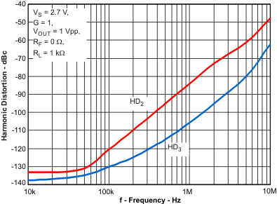
- HD2, HD3: –85 dBc, –105 dBc at 1 MHz (2 VPP)
- Input Voltage Noise: 4.6 nV/√Hz (f = 100 kHz)
- Input Offset Voltage: 65 µV (±400-µV Max)
- CMRR: 116 dB
- Output Current Drive: 50 mA
- RRO: Rail-to-Rail Output
- Input Voltage Range: –0.2 V to +3.9 V
(5-V Supply)
2 Applications
- Low-Power Signal Conditioning
- Audio ADC Input Buffers
- Low-Power SAR and ΔΣ ADC Drivers
- Portable Systems
- Low-Power Systems
- High-Density Systems
3 Description
The OPA2836-Q1 device is a dual-channel, ultra-low power, rail-to-rail output, negative-rail input, voltage-feedback operational amplifier designed to operate over a power-supply range of 2.5 V to 5.5 V (single supply), or ±1.25 V to ±2.75 V (dual supply). Consuming only 1 mA per channel with a unity-gain bandwidth of 205 MHz, this amplifier sets an industry-leading, power-to-performance ratio for rail-to-rail amplifiers.
For battery-powered, portable applications where power is a key importance, the low-power consumption and high-frequency performance of the OPA2836-Q1 offers designers performance-versus-power that is not attainable in other devices.
The OPA2836-Q1 is characterized for operation over the extended industrial temperature range of –40°C to +125°C.
Device Information(1)
| PART NUMBER | PACKAGE | BODY SIZE (NOM) |
|---|---|---|
| OPA2836-Q1 | VSSOP (8) | 3.00 mm × 3.00 mm |
- For all available packages, see the orderable addendum at the end of the data sheet.
Harmonic Distortion vs Frequency

4 Revision History
| DATE | REVISION | NOTES |
|---|---|---|
| December 2016 | * | Initial release. |