SLVSAD4B August 2010 – April 2015 TPS22934
PRODUCTION DATA.
- 1 Features
- 2 Applications
- 3 Description
- 4 Revision History
- 5 Pin Configuration and Functions
-
6 Specifications
- 6.1 Absolute Maximum Ratings
- 6.2 ESD Ratings
- 6.3 Recommended Operating Conditions
- 6.4 Thermal Information
- 6.5 Electrical Characteristics
- 6.6 Switching Characteristics: VIN = 3.6 V
- 6.7 Switching Characteristics: VIN = 2.5 V
- 6.8 Switching Characteristics: VIN = 1.8 V
- 6.9 Switching Characteristics: VIN = 1.5 V
- 6.10 Typical Characteristics
- 7 Parameter Measurement Information
- 8 Detailed Description
- 9 Applications and Implementation
- 10Power Supply Recommendations
- 11Layout
- 12Device and Documentation Support
- 13Mechanical, Packaging, and Orderable Information
Package Options
Mechanical Data (Package|Pins)
- YZV|4
Thermal pad, mechanical data (Package|Pins)
Orderable Information
1 Features
- Integrated Single Channel Load Switch
- Input Voltage: 1.5 V to 3.6 V
- ON-Resistance
- rDS(ON) = 63 mΩ at VIN = 3.6 V
- rDS(ON) = 69 mΩ at VIN = 2.5 V
- rDS(ON) = 78 mΩ at VIN = 1.8 V
- rDS(ON) = 87 mΩ at VIN = 1.5 V
- 1-A Maximum Continuous Switch Current
- Integrated Hysteresis Enable Input (ON Pin) Allows Easy Power-Rail Sequencing
- Controlled Slew Rate Option: 26 µs at 3.6 V
- Quick Output Discharge Transistor
- Ultra-Small CSP-4 Package
- ESD Performance Tested Per JESD 22
- 3000-V Human-Body Model
(A114-B, Class II) - 1000-V Charged-Device Model (C101)
- 3000-V Human-Body Model
2 Applications
- Battery-Powered Equipment
- Portable Industrial Equipment
- Portable Medical Equipment
- Portable Media Players
- Point-of-Sales Terminals
- GPS Devices
- Digital Cameras
- Portable Instrumentation
- Smart Phones
3 Description
The TPS22934 is a small, low ON-resistance (rON) load switch with controlled turnon. The devices contain a P-channel MOSFETs that can operate over an input voltage range of 1.5 V to 3.6 V.
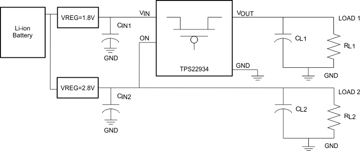
The switch is controlled by an ON/OFF input (ON), which has built-in hysteresis (VTH+(typ) = 2.35 V) allowing an easy use of TPS22934 in power-rail sequencing applications.
In the TPS22934 a 35-Ω on-chip load resistor is added for output quick discharge when switch is turned off.
In the TPS22934, the rise time of the device is internally controlled to avoid inrush current. The TPS22934 features a typical rise time of 26 µs with a 3.6-V input.
The the TPS22934 is available in an ultra-small space-saving 4-pin CSP package and is characterized for operation over the free-air temperature range of –40ºC to 85ºC.
Device Information(1)
| PART NUMBER | PACKAGE | BODY SIZE (NOM) |
|---|---|---|
| TPS22934 | DSBGA (4) | 0.90 mm × 0.90 mm |
- For all available packages, see the orderable addendum at the end of the data sheet.
Typical Application
1.8-V Power-Rail Sequencing
