SLVS957E June 2009 – April 2016 TPS61300 , TPS61301 , TPS61305
PRODUCTION DATA.
- 1 Features
- 2 Applications
- 3 Description
- 4 Revision History
- 5 Device Comparison Table
- 6 Pin Configuration and Functions
- 7 Specifications
-
8 Detailed Description
- 8.1 Overview
- 8.2 Functional Block Diagrams
- 8.3
Feature Description
- 8.3.1 Safety Timer Accuracy
- 8.3.2 LED Failure Modes and Overvoltage Protection
- 8.3.3 Start-Up Sequence
- 8.3.4 Power Good (Flash Ready)
- 8.3.5 LED Temperature Monitoring (TPS61305, TPS61305A, TPS61306)
- 8.3.6 Hot Die Detector
- 8.3.7 NRESET Input: Hardware Enable and Disable
- 8.3.8 ENDCL Input: DC Light Hardware Control
- 8.3.9 Flashlight Blanking (Tx-MASK)
- 8.3.10 Undervoltage Lockout
- 8.3.11 Storage Capacitor Active Cell Balancing
- 8.3.12 RED Light Privacy Indicator
- 8.3.13 White LED Privacy Indicator
- 8.3.14 Storage Capacitor, Precharge Voltage Calibration
- 8.3.15 Storage Capacitor, Adaptive Precharge Voltage
- 8.3.16 Serial Interface Description
- 8.4
Device Functional Modes
- 8.4.1 Down-Mode in Voltage Regulation Mode
- 8.4.2 LED High-Current Regulators, Unused Inputs
- 8.4.3 Power-Save Mode Operation, Efficiency
- 8.4.4 Mode of Operation: DC Light and Flashlight
- 8.4.5 Flash Strobe is Level Sensitive (STT = 0): LED Strobe Follows FLASH_SYNC Input
- 8.4.6 Flash Strobe Is Leading Edge Sensitive (STT = 1): One-Shot LED Strobe
- 8.4.7 Current Limit Operation
- 8.4.8 Hardware Voltage Mode Selection
- 8.4.9 Shutdown
- 8.4.10 Thermal Shutdown
- 8.4.11 F/S-Mode Protocol
- 8.4.12 HS-Mode Protocol
- 8.4.13 TPS6130xx I2C Update Sequence
- 8.5
Register Maps
- 8.5.1 Slave Address Byte
- 8.5.2 Register Address Byte
- 8.5.3 REGISTER1 (TPS61300, TPS61301)
- 8.5.4 REGISTER1 (TPS61305, TPS61305A, TPS61306)
- 8.5.5 REGISTER2 (TPS61300, TPS61301)
- 8.5.6 REGISTER2 (TPS61305, TPS61305A, TPS61306)
- 8.5.7 REGISTER3
- 8.5.8 REGISTER4
- 8.5.9 REGISTER5
- 8.5.10 REGISTER6 (TPS61300, TPS61301)
- 8.5.11 REGISTER6 (TPS61305, TPS61305A)
- 8.5.12 REGISTER7
-
9 Application and Implementation
- 9.1 Application Information
- 9.2 Typical Applications
- 9.3
System Examples
- 9.3.1 2x 600-mA High-Power White LED Solution Featuring Privacy Indicator
- 9.3.2 White LED Flashlight Driver and Audio Amplifier Power Supply Operating Simultaneously
- 9.3.3 White LED Flashlight Driver and Audio Amplifier Power Supply Operating Simultaneously
- 9.3.4 White LED Flashlight Driver and Audio Amplifier Power Supply Exclusive Operation
- 9.3.5 White LED Flashlight Driver and Auxiliary Lighting Zone Power Supply
- 9.3.6 TPS61300, Typical Application
- 9.3.7 TPS61301, Typical Application
- 9.3.8 TPS61305 Typical Application
- 9.3.9 TPS61306, Typical Application
- 10Power Supply Recommendations
- 11Layout
- 12Device and Documentation Support
- 13Mechanical, Packaging, and Orderable Information
Package Options
Mechanical Data (Package|Pins)
- YFF|20
Thermal pad, mechanical data (Package|Pins)
Orderable Information
1 Features
- Four Operational Modes
- DC Light and Flashlight
- Voltage Regulated Converter: 3.8 V to 5.7 V
- Standby: 2 μA (Typical)
- Storage Capacitor Friendly Solution
- Automatic VF and ESR Calibration
- Power-Save Mode for Improved Efficiency at Low Output Power, Up to 95% Efficiency
- Output Voltage Remains Regulated When Input Voltage Exceeds Nominal Output Voltage
- I2C Compatible Interface up to 3.4 Mbits/s
- Zero Latency Tx-Masking Input
- Hardware Voltage Mode Selection Input (TPS61300, TPS61301)
- DC Light Mode Selection Input
(TPS61300, TPS61306) - Hardware Reset Input (TPS61301, TPS61305)
- LED Temperature Monitoring (TPS61305)
- Privacy Indicator LED Output
- Integrated LED Safety Timer
- Total Solution Size of Less Than 25 mm2 (< 1 mm height)
- Available in a 20-Pin NanoFree™ (DSBGA)
2 Applications
- Single, Dual, or Triple White LED Flashlight Supply for Cell Phones and Smart-Phones
- LED Based Xenon Killer Flashlight
- Audio Amplifier Power Supply
3 Description
The TPS6130xx device is based on a high-frequency synchronous boost topology with constant current sinks to drive up to three white LEDs in parallel (400‑mA, 800-mA, and 400-mA maximum flash current). The extended high-current mode (HC_SEL) allows up to 1025-mA, 2050-mA, and 1025-mA flash current out of the storage capacitor.
The high-capacity storage capacitor on the output of the boost regulator provides the high-peak flash LED current, thereby reducing the peak current demand from the battery to a minimum.
The 2-MHz switching frequency allows the use of small and low profile 2.2-μH inductors. To optimize overall efficiency, the device operates with a 400-mV LED feedback voltage.
The TPS6130xx device not only operates as a regulated current source, but also as a standard voltage boost regulator. The device keeps the output voltage regulated even when the input voltage exceeds the nominal output voltage. The device enters power-save mode operation at light load currents to maintain high efficiency over the entire load current range.
To simplify flashlight synchronization with the camera module, the device offers a trigger pin (FLASH_SYNC) for zero latency LED turnon time.
Table 1. Device Information(1)
| PART NUMBER | PACKAGE | BODY SIZE (NOM) |
|---|---|---|
| TPS6130xx | DSBGA (20) | 1.90 mm × 2.20 mm |
- For all available packages, see the orderable addendum at the end of the data sheet.
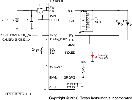
3.1 Simplified Schematic
